1. Introduction
Welcome to the YGN Effects Framework documentation! This guide will walk you through every step of populating your pedal’s Printed Circuit Board (PCB) with all its electronic components. To get started, we will be assembling the Small IO Board. It’s a quick and simple build, making it the perfect introduction to the process.
The techniques and methods you learn here are universal across our entire range of PCBs. Whether you’re building a simple fuzz or a complex digital effect, the core skills are exactly the same. Let’s get our tools ready!
A friendly note on SMT
If you’ve only ever worked with larger, through-hole components, the idea of handling tiny Surface-Mount Technology (SMT) parts might seem a bit intimidating. But we’re going to use a technique that makes it surprisingly simple: hot plate reflow soldering.
This method involves applying solder paste with a stencil and letting a controlled heat source do all the work. It’s an incredibly forgiving process, as the surface tension of the molten solder naturally pulls components into perfect alignment. We chose SMT for our framework because it allows for simpler, cleaner circuit routing. Best of all, this process results in a beautiful, professional-looking board that requires no cleaning and that can be easily reworked with a hot-air station.
We’ll guide you through each step. Take your time, and you’ll be an SMT pro before you know it.
2. Required Tools and Materials
Here is everything you’ll need to assemble your PCB.
- A YGN Effects PCB: The foundation of your build!
- Solder Paste Stencil: This is essential for applying the paste accurately. You can have one professionally fabricated using the Gerber files for your board, or mill your own from a plastic sheet on a CNC.
- Solder Paste: We highly recommend Chipquik SMD291SNL50T3. It’s just great: it has a long shelf life, is perfectly usable even past its expiration date, doesn’t need to be refrigerated and is truly “no-clean.”
- Squeegee: You need something flat and firm to spread the paste. An old credit card works perfectly for this.
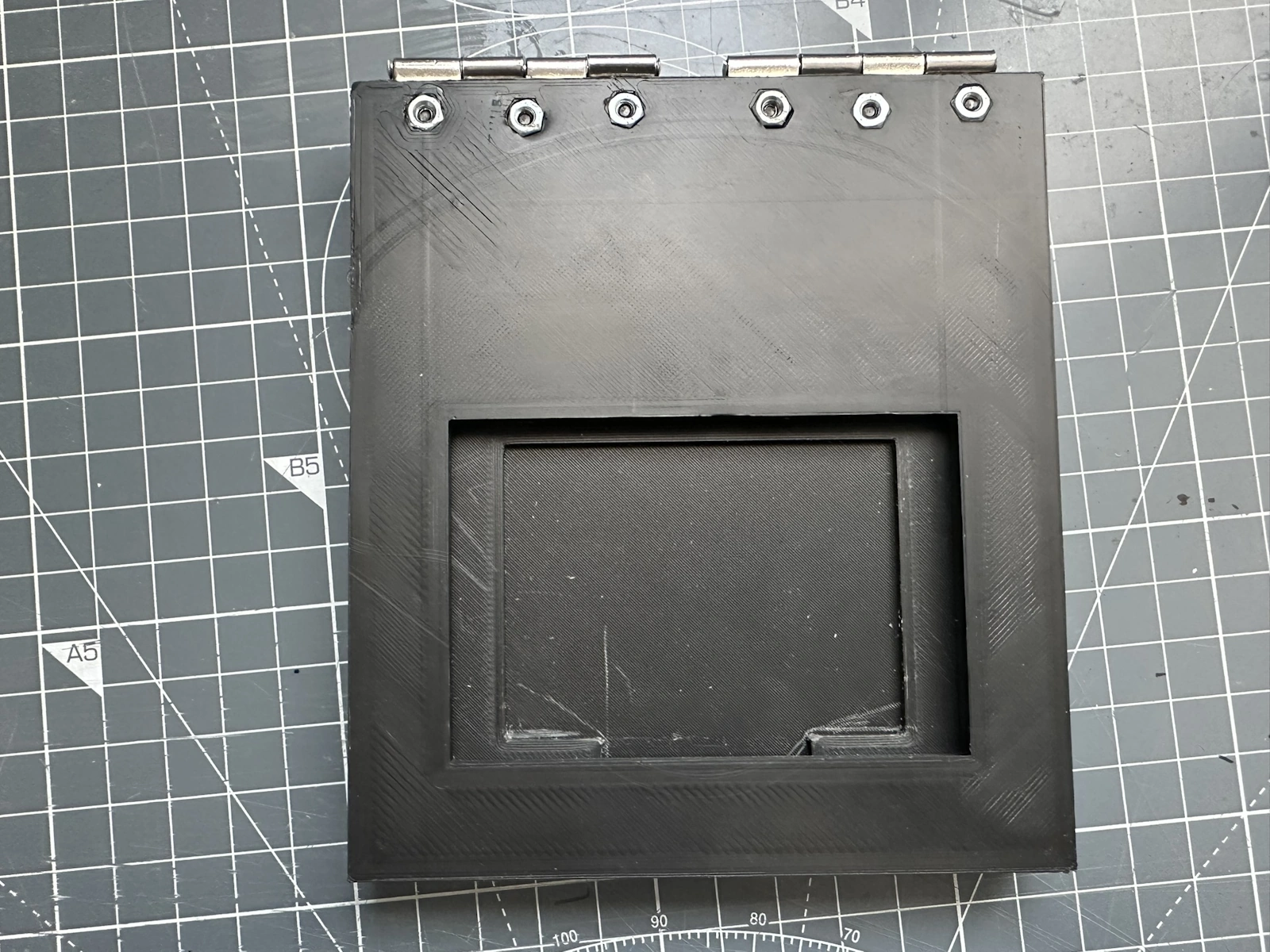
- Stencil Jig: Our custom-designed, 3D-printed stencil holder will make the process much easier. Build your own with the Stencil Holder Assembly guide.
- Tweezers: You’ll need these to place the components. It’s best to have a few different sizes and head types. Small, pointy tweezers are great for tiny resistors and capacitors, while larger ones can be better for handling ICs. Finding the right tweezers is a very personal choice and may take some trial and error.
- Reflow Hot Plate: This is what will heat the board and melt the solder. Many commercial and DIY versions are available in various sizes.
- Isopropyl Alcohol (IPA) and Paper Towels: For cleaning the stencil and any accidental messes.


3. Applying the Solder Paste
With our workspace ready, it’s time for the most crucial step. Take your time here—a good paste application makes the rest of the process a breeze.
- Clean the board and stencil. Before you begin, give the PCB and the stencil a quick wipe with Isopropyl Alcohol (IPA) and a paper towel. This removes any oils or dust and ensures the paste sticks only where it should.
- Prepare the paste. Solder paste is fine sitting in the jar for a while, but give it a thorough stir before each use to recombine the metal particles and flux. Then scoop a small amount out of its container and spread a thick line of it along one edge of your squeegee (e.g., a credit card). A toothpick or a small spatula works well for this.
- Spread the paste. Press the squeegee flat against the stencil and drag it across the openings to fill them completely. Then, make another pass holding the squeegee at a 45° angle. This scrapes the excess paste off the stencil and back onto the squeegee. Repeat this process a few times to ensure every pad is perfectly filled.
- Make a final pass. Perform one last, clean pass at a 45° angle to remove as much excess paste from the stencil surface as possible.
- Save the excess. Scrape the remaining solder paste from your squeegee and return it to the jar. A little goes a long way!
- Remove the stencil. This is a key moment. Lift the stencil straight up off the PCB in one smooth, decisive motion. Avoid letting it slide, as this can smear the paste. If you’re using the Stencil Holder jig, this part is effortless — simply opening the holder pops the stencil off the PCB instantly, giving you a clean separation with no risk of smearing. The goal is a clean “pop-off” that leaves behind perfectly formed paste deposits.
- Clean your tools. Immediately clean your stencil and squeegee with IPA and paper towels. Dried solder paste is much harder to remove.
- Inspect your work. Look closely at the PCB. All the pads should be covered with a uniform, gray deposit of solder paste.
Tip: If some pads look thin or you see bridges between pads, don’t worry! You can simply place the PCB back in the jig, lay the stencil back on top (it should snap into place), and repeat the application process. The same “pop-on, pop-off” motion works wonders here.


4. Placing the Components
This is where your circuit starts to come to life! A bit of organization now will make the whole process much faster and more enjoyable.
Preparation is Key
-
Organize Your Components: Working from cut tapes of tiny components is not practical. We strongly recommend a good storage system. There are many options, from simple trays to multi-drawer bins. We personally use and love the AideTek BOX-ALL system, with separate organizers for resistors, capacitors, ICs, etc. A neat, logical organization will significantly speed up your build.


- Know What Goes Where: While you can use the Bill of Materials (BOM) and the silk screen overlay on the PCB, the small size of the components can sometimes make the overlay hard to read. For a crystal-clear view, we recommend opening the mechanical layer file from the effect’s repository. This file shows only the component outlines and their designators.
Tip: Feel free to print this mechanical layer view and annotate it with component values. There’s usually plenty of space, and it creates a perfect “map” for your build.
- Clean Your Tweezers: Your tweezers must be perfectly clean and have sharp, well-aligned tips. Tiny 0603 components are so light that any residue or slight deformation on the tweezer tips can cause the part to stick or be misplaced.


The Placement Process
-
Place the components. With your parts organized and your placement map ready, it’s time to start. The general strategy is to work from the smallest components up to the largest.
Note: Don’t stress about getting the placement absolutely perfect! The magic of the reflow process is that the surface tension of the molten solder (capillary action) will pull most components into precise alignment. Just get them reasonably centered on their pads.
A good workflow is:
- Start with 0603 resistors. Pick one value (e.g., 10kΩ), and place all of them on the board. Move to the next value and repeat.
- Move to 0603 capacitors. Follow the same process.
- Continue with larger passives (0805, 1206, etc.).
- Next, place diodes and transistors, from smallest to largest. Pay close attention to their orientation!
- Then, place the Integrated Circuits (ICs).
- Finally, place the “big stuff” like electrolytic capacitors, relays, or other bulky parts.


5. The Reflow Process
This is the magic moment where all the separate parts become one solid circuit.
Understanding the Reflow Profile
Solder paste manufacturers provide a “reflow profile,” which is a graph of temperature over time. It’s designed to ensure a strong and reliable solder joint. The process has three main stages:
- Ramp-up (or Pre-heat): The temperature slowly rises to activate the flux in the solder paste. The flux cleans the metal surfaces of the components and pads.
- Soak: The temperature is held steady. This allows the flux to spread and ensures the entire board and all its components reach a uniform temperature.
- Reflow: The temperature is quickly raised above the solder’s melting point. The solder liquefies, flows, and forms permanent connections.
We will follow this profile closely for the first two phases. For the final reflow phase, we’ll rely on visual cues, as most hobbyist hot plates can’t precisely match the steep temperature curves.

Let’s Reflow!
- Prepare for landing. Before you start heating, plan how you will remove the hot PCB from the plate. You’ll need a tool (like flat pliers or sturdy tweezers) and a heat-resistant surface (like a piece of scrap wood or a copper sheet) for the board to cool on. Rehearse the motion of picking up the board and placing it on the cooling spot. The solder will be liquid, so a smooth, steady hand is crucial to avoid dislodging components.
- Place the board. Gently place your populated PCB in the center of the cold hot plate.
- Ramp-up. Set your hot plate to 150°C and start a timer. Wait for approximately 90 seconds.
- Soak. Increase the temperature setting to 180°C. Wait for another 90 seconds. During this phase, you’ll see the solder paste change in appearance from a dull gray to a slightly shinier, wet look. You may also see a small amount of smoke as the flux and solvents activate and burn off. This is normal!
- Reflow! Turn the hot plate up to its maximum setting (e.g., 250°C). Now, watch the board closely. As the temperature rises past ~240°C, the magic will happen. You’ll see the solder paste instantly transform into shiny, liquid silver. Wait until you see this happen on every single pad. The pads for larger components (like electrolytic capacitors) will be the last to melt. Once everything is shiny, execute your plan: smoothly lift the board off the plate and place it on your cooling surface.
- Inspect the joints. After the board has cooled completely (wait at least 5-10 minutes), it’s time to inspect your work. Grab a magnifier if you have one and look at the solder joints.
Tip: A good SMT solder joint, called a “fillet,” should be shiny and have a concave shape where the solder has wicked up from the pad onto the component’s lead. This indicates a strong, reliable connection. Check for any bridges (solder connecting two pads that shouldn’t be) or unsoldered pads.


6. Testing Your Board
Once all the through-hole components (like headers and connectors) have been soldered, you’re ready to power up the board and confirm everything is working correctly.
- Locate the Test Points: The PCB has several designated test points, clearly labeled on the silkscreen overlay (e.g., “TP1”, “TP2”).
- Find the Expected Values: To know what you’re looking for, refer to the Test Points document located in the fabrication output folder within each effect’s repository. This document lists each test point and its expected voltage or behavior.
- Measure the Voltages: Power up the board. To take a measurement, you’ll need a multimeter. All of the un-tented vias (the small, exposed copper holes) running along the edges of the board are connected to the ground plane. These make a perfect, stable anchor point for the black COM probe of your multimeter. Touch the red probe to each test point and compare the reading on your multimeter to the value listed in the documentation. If everything matches, congratulations on a successful build!

Found an Issue?
Help improve this documentation by reporting errors or suggesting improvements.