Introduction
Welcome to the YGN Effects Framework documentation! The Small IO Board carries a small switching power supply stage built around the ICL7660S charge-pump IC, and it’s designed to be flexible: the same PCB can be stuffed to deliver -9V, +18V or ±15V on top of the standard +9V supply, depending on what the effect circuit plugged into it actually needs.
There’s no extra hardware to source and no cutting traces involved. Every footprint for every variant already exists on the board, so building the one you want is simply a matter of populating the right handful of parts and leaving the rest empty. This guide walks you through picking a variant and stuffing it correctly.
Note: This guide assumes you’re already comfortable with the general SMD population process. If you haven’t yet, read the SMD PCB Assembly guide first: everything here builds on that same technique, just applied to one specific area of the board.
How the Switching Stage Works
The whole trick lives around IC1, an ICL7660S. On its own, this chip is a “charge pump”: it uses an internal oscillator to flip a capacitor back and forth many thousands of times a second, moving charge around to turn one DC voltage into another. Fed from the board’s protected +9V rail (labelled +REG on the schematic), it can either invert that voltage to make a negative rail, or double it to make a higher positive rail. The diodes and capacitors clustered around IC1 (D2-D6 and C6-C11) shape which of those two things happens, and the resistor footprints RJ1-RJ4 tie off whichever rail your chosen variant doesn’t use, so nothing is left floating.
IC1 and C5 (its input decoupling capacitor) are common to all three variants and are always populated. Everything else in this stage is optional, and which parts you stuff depends entirely on the variant you’re building.
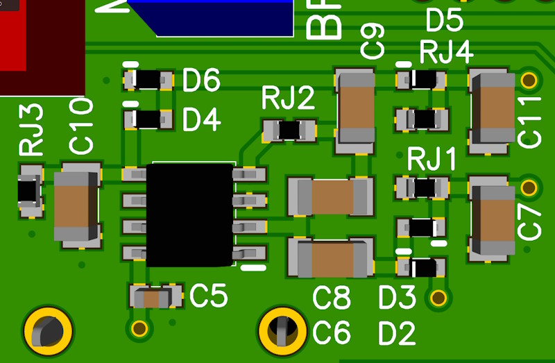
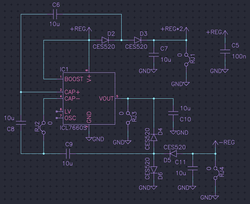
Tip: IC1’s BOOST pin (pin 1) is tied to V+ in every variant. This pushes the internal oscillator up to around 35kHz, well above the audio band, so switching noise doesn’t make its way into your effect’s signal path.
Choosing Your Variant
The J2 header, which powers the effect PCB plugged into your IO board, always exposes three rails: +REG, +REG*2 and -REG. +REG is a straight pass-through of your +9V input, so it’s always present no matter which variant you build. +REG*2 and -REG are the “choose your own adventure” pair: what each one actually carries depends entirely on which variant you populate, and that’s what the table below sets out.
| Variant | +REG*2 | -REG | Typical use case |
|---|---|---|---|
| -9V | Unused (grounded) | -9V | Dual-supply op-amp circuits built around a standard ±9V split with +REG. |
| +18V | +18V | Unused (grounded) | Single-supply circuits that want extra headroom over a plain 9V. |
| ±15V | +15V | -15V | Op-amp circuits designed around a standard ±15V audio supply, for the most headroom of the three. |
Caution: Populate exactly one column, fully. Mixing parts from two different variants, or only half-populating one, can feed the wrong voltage into whatever effect PCB is plugged into J2 and damage it. If you’re not sure which variant your effect circuit needs, check its documentation before you start soldering.
Populating The Board
Populating: -9V
This is the simplest variant: IC1 runs as a straightforward voltage inverter, giving you a standard ±9V split supply.
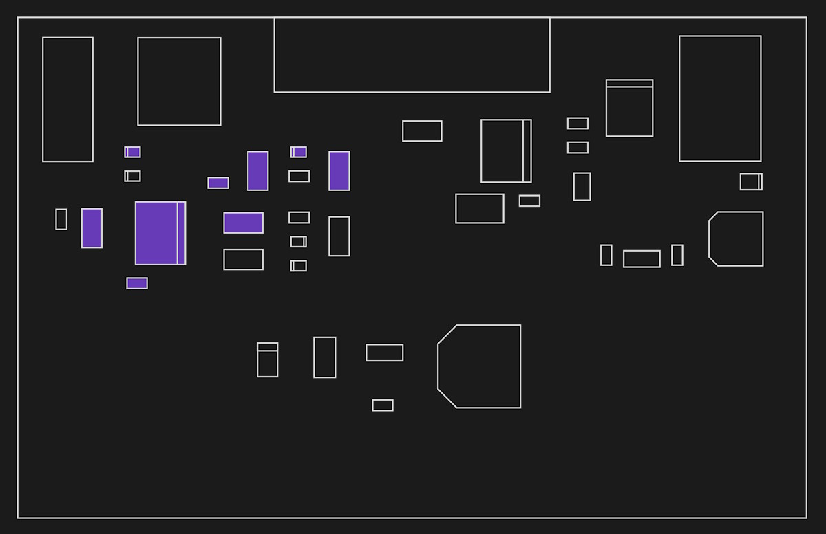
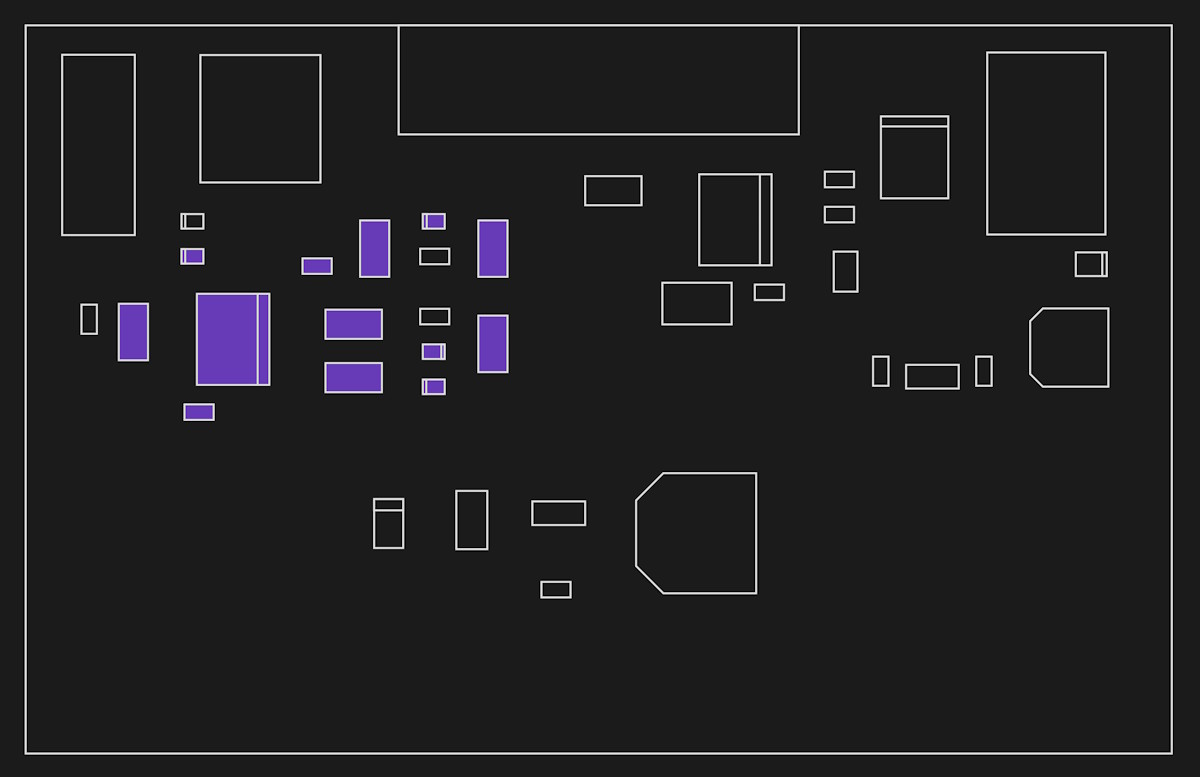
- Populate C8, RJ2, C10, C9, D5, C11 and D6.
- Leave empty C6, D2, D3, C7, D4, RJ1, RJ3 and RJ4.
Note: D6 clamps -REG to ground-referenced ≈ -9V. It’s what keeps your negative rail sitting at roughly the same magnitude as +REG.
Populating: +18V
Here IC1 is used purely as a square-wave generator: it doesn’t invert anything itself, it just drives an external doubler pump built from D2, D3 and their capacitors.
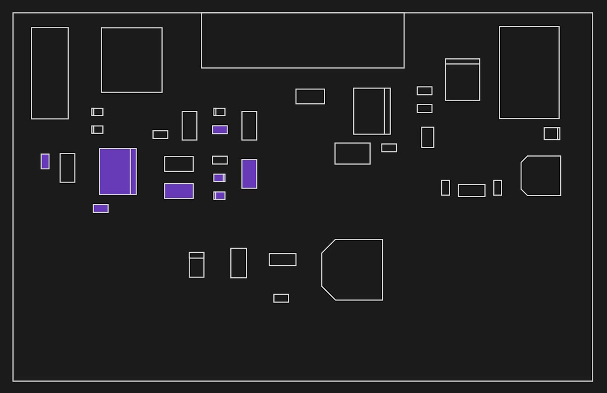
- Populate C6, D2, D3, C7, RJ3 and RJ4.
- Leave empty C8, RJ2, C9, C10, C11, D4, D5 and D6.
Note: RJ3 and RJ4 tie the unused VOUT pin and the unused -REG rail to ground. Since this variant doesn’t produce a negative rail, those two footprints matter just as much as the ones that do the doubling.
Populating: ±15V
This variant runs both pumps at once: the doubler feeds a cascaded inverter stage, giving you a split supply with more headroom than the -9V variant.
- Populate C6, D2, D3, C7, C8, RJ2, C10, C9, D5, C11 and D4.
- Leave empty D6, RJ1, RJ3 and RJ4.
Note: D4 and D6 are mutually exclusive. This variant uses D4, not D6, don’t populate both. Doing so clamps the negative pump to ground and drags -REG back up to roughly -8V instead of the intended ±15V.
Verifying Your Output Voltages
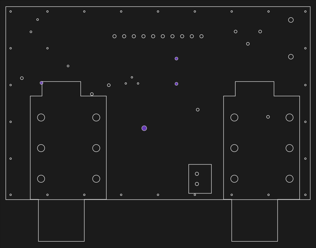
Once your board is soldered, it’s worth confirming the switching stage is producing what you expect before you plug an effect PCB into J2. The board has dedicated test points for exactly this: TP1 (+REG), TP3 (+REG*2) and TP4 (-REG).
- Power the board from a standard 9V supply.
- Flip the board over to the bottom, copper side. The test points are vias accessed from this side, and they’re labelled right there on the silkscreen.
- Set your multimeter to DC volts and connect its black probe to one of the board’s ground vias.
- Measure TP1 (+REG). You should read approximately +9V on every variant, this rail simply passes the input supply through.
- Measure TP3 (+REG*2) and TP4 (-REG) and compare against the table below.
Tip: Probing from the bottom side is not just convenient, it’s safer. There are no SMT components on this face of the board, so there’s no risk of your probe tip slipping and bridging two component pins together.
| Variant | TP3 (+REG*2) | TP4 (-REG) |
|---|---|---|
| -9V | ≈ 0V (tied to ground by RJ1) | ≈ -9V |
| +18V | ≈ +17V unloaded | ≈ 0V (tied to ground by RJ4) |
| ±15V | ≈ +17V unloaded | ≈ -17V unloaded |
Note: The doubled rails read a little under their nameplate voltage even unloaded, because of diode drops through the pump network. Once you connect a real effect circuit drawing a few mA, expect the ±15V variant to settle closer to its name, around ±15V. A 0V reading on the rail your variant intentionally grounds isn’t a fault, that’s RJ1 or RJ4 doing its job.
If a rail reads far outside these ranges, double-check the populate/leave-empty lists for your chosen variant against the section above before you go any further.
That’s it, your Small IO Board’s power supply is built, verified and ready to feed whatever effect circuit you connect to it.
Found an Issue?
Help improve this documentation by reporting errors or suggesting improvements.